
Digital Design and Computer Organization
COPY PASTE FOLLOWING LINK IN BROWSER FOR 1ST LAB - INTRODUCTION
https://www.slideshare.net/GururajSurampalli/analog-and-digital-electronics-lab
MODULE 1
EXPERIMENT 1
AIM: Simulate BJT CE voltage divider biased voltage amplifier using any suitable circuit simulator


EXPERIMENT 2
2. Using ua 741 Opamp, design a 1 kHz Relaxation Oscillator with 50% duty cycle. And simulate the same.


wave forms

THEORY:
AIM: To design and implement a rectangular waveform generator (op-amp relaxation
oscillator) for a given frequency.
COMPONENTS REQUIRED: Op-amp μA 741, Resistor of 4.7KΩ, 6.8KΩ, 10KΩ
Potentiometer, A capacitor of 0.1 μF(104), Regulated DC power supply, CRO


wave forms

THEORY:
Op-Amp Relaxation Oscillator is a simple Square wave generator which is also called as a Free running oscillator or Astable multivibrator or Relaxation oscillator. In this figure, the op-amp operates in the saturation region. Here, a fraction (R1/ (R1+R2)) of output is fed back to the noninverting input terminal. Thus reference voltage is (R1/ (R1+R2)) Vo. And may take values as + (R1/ (R1+R2)) Vsat or - (R1/ (R1+R2)) Vsat. The output is also fed back to the inverting input terminal after integrating by means of a low-pass RC combination. Thus whenever the voltage at the inverting input terminal just exceeds reference voltage, switching takes place resulting in a square wave output.
PROCEDURE:
1. Before making the connections check all the components using a multimeter.
2. Make the connections as shown in figure and switch on the power supply.
3. Observe the voltage waveform across the capacitor on CRO.
4. Also observe the output waveform on CRO. Measure its amplitude and frequency.
RESULT:
The frequency of the oscillations = ___ Hz.

SIMULATION


WAVEFORMS

The above simulation is performed on MultisimLive, Click on following link to observe output
https://www.multisim.com/content/AryKBUPadVRMMndVYiyUCY/relaxation-oscillator/open/
Click Play button to simulate and Click on Grapher to see waveform
https://www.multisim.com/content/AryKBUPadVRMMndVYiyUCY/relaxation-oscillator/open/
Click Play button to simulate and Click on Grapher to see waveform
EXPERIMENT 3
Aim: Design an astable multivibrator circuit for three cases of duty cycle (50%, <50% and >50%)
using NE 555 timer IC. Simulate the same for anyone duty cycle
COMPONENTS
REQUIRED:
555 Timer IC, Resistors of 3.3KΩ, 6.8KΩ, Capacitors of 0.1μF,
0.01 μF, Regulated power supply, CRO


NOTE: 1.When RA<<RB, D approaches 50%
2. When RA>>RB, D approaches 100%
Circuit Diagram:

WAVEFORMS

NOTE: FOR 50% connect RB from pin 2 to pin 3
FOR <50% connect diode across RB resistor
FOR <50% connect diode across RB resistor
PROCEDURE:
1.
Before making the connections, check the components using a multimeter.
2.
Make the connections as shown in figure and switch on the power
supply.
3.
Observe the capacitor voltage waveform at 6th pin of 555 timer on
CRO.
4.
Observe the output waveform at 3rd pin of 555 timer on CRO (shown
below).
5.
Note down the amplitude levels, time period and hence calculate duty
cycle.
Simulate by clicking
endmodule
THEORY:
Multivibrator
is a form of an oscillator, which has a non-sinusoidal output. The
output waveform is rectangular. The multivibrators are classified as:
Astable
or free-running multivibrator:
It alternates automatically between two states (low and high for a
rectangular output) and remains in each state for a time-dependent
upon the circuit constants. It is just an oscillator as it requires
no external pulse for its operation. Monostable
or one-shot multivibrator:
It has one stable state and one quasi-stable. The application of an
input pulse triggers the circuit time constants. After a period of
time determined by the time constant, the circuit returns to its
initial stable state. The process is repeated upon the application of
each trigger pulse. Bistable
Multivibrators:
It has both stable states. It requires the application of an external
triggering pulse to change the output from one state to another. After
the output has changed its state, it remains in that state until the
application of next trigger pulse. The flip flop is an example.
RESULT:
TH=-------------
TL
= ------------
T
= -------------
The
frequency of the oscillations = 1/T= ___ Hz.
%Duty
cycle (DC) = tH/T*100 = ----------
SIMULATION USING MULTISIM

waveform

EXPERIMENT 4
Using ua 741 opamap, design a window comparator for any given UTP and LTP. And
simulate the same.
AIM:
• To design a window comparator for any given UTP and LTP
• To simulate the same
COMPONENTS REQUIRED: ua 741, Resistors 10K, 4.7K, function generator, power supply, Oscilloscope, wires etc
Theory
• A comparator is a circuit which compares a signal voltage applied at one input of an opamp
with a known reference voltage at the other input.
• A window comparator is basically the inverting and the non-inverting comparators,
combined into a single comparator stage. The window comparator detects input voltage
levels that are within a specific band or window of voltages, instead of indicating whether a
voltage is greater or less than some preset or fixed voltage reference point.
• In window comparator, the output changes state when the input voltage goes above or
below the reset reference voltage. In a window comparator, there are two reference voltages,
called lower and upper trip points (UTP & LTP). Output is in one state, when it is inside the
window created by the lower and the upper trip points and in the other state when it is
outside the window.
DESIGN:
Design goals: UTP = 3.33V, LTP = 1.66V
A reference voltage, VCC , is divided down by resistors R1-R3. The two node voltages, UTP and
LTP, define the upper window voltage and lower window voltage, respectively. When the input
voltage is between UTP and LTP, the output is ‘HIGH’, or VP ; when outside the window voltage,
the output is pulled down to 0V. Equations (1) and (2) define UTP and LTP, respectively:

Choose R1=R2=R3=R=10K ohm Rp=4.7K ohm Vcc=5V

PROCEDURE:
1. Before making the connections check all the components using a multimeter.
2. Make the connections as shown in figure and switch on the power supply.
3. Observe the voltage waveform across the capacitor on CRO.
4. Also observe the output waveform on CRO. Measure its amplitude and frequency.
RESULT:
Theoretical LTP = ___ V.
Theoretical UTP = ___ V.
Practical LTP= ___ V
Practical UTP= ___ V


Click Play button to simulate and Click on Grapher to see waveform
HA FA HS FS Using XOR Gates


Experiment 2: Design and implement code converter I) Binary to Gray (II) Gray to Binary Code
Theoretical UTP = ___ V.
Practical LTP= ___ V
Practical UTP= ___ V
SIMULATION

WAVEFORMS

The above simulation is performed on MultisimLive, Click on following link to observe output
Click Play button to simulate and Click on Grapher to see waveform
MODULE 2
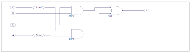
Experiment 1:
Given a 4-variable logic expression, simplify it using appropriate technique and inplement the
same using basic gates.

EXPERIMENT: [NOT IN SYLLABUS] here https://drive.google.com/file/d/1MX8f8XxUvscAaRqZmt8fXnJXMNbMzIuw/view?usp=sharing
HA FA HS FS Using XOR Gates
MODULE 3
Experiment 1:Given a 4-variable logic expression, simplify it using appropriate technique and realize the simplified logic expression using 8:1 multiplexer IC.
For Practice 


Experiment 2: Design and implement code converter I) Binary to Gray (II) Gray to Binary Code
Click For Experiment: https://drive.google.com/file/d/1JhwCyJLLpQOmBjn9sg7sRJOyU_2BkbFi/view?usp=sharing


Output

EXPERIMENT 2


or


For details click the link below
MODULE 4
EXPERIMENT 1
Given a 4-variable logic expression, simplify it using appropriate technique and simulate the
same in HDL simulator
Program
Output
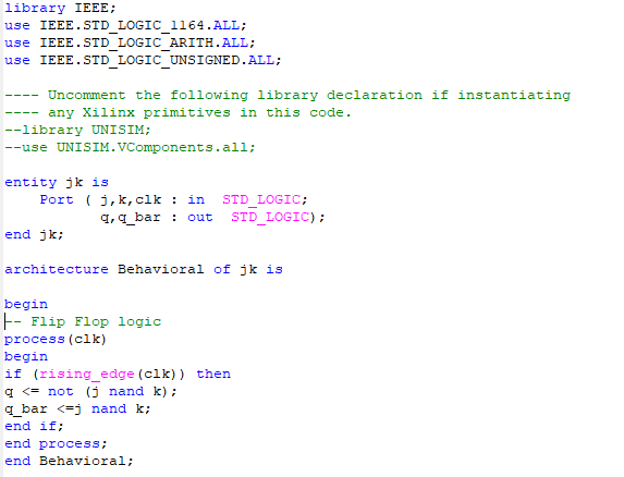
EXPERIMENT 2
Realize a J-K Master / Slave Flip-Flop using NAND gates and verify its truth table. And
implement the same in HDL.
or
VHDL CODE JK FF AND JK MS FF:https://drive.google.com/file/d/198c-bRFM8y9dx-mAZ24JinezzgwgnL6G/view?usp=sharing
MODULE 5
EXPERIMENT 1
AIM: Design and implement a mod-n (n<8) synchronous up counter using J-K Flip-Flop ICs and
demonstrate its working.
For details click the link below
EXPERIMENT 2
AIM: Design and implement an asynchronous counter using decade counter IC to count up from 0 to
n (n<=9) and demonstrate on 7-segment display (using IC-7447)
Experiments Beyond Curriculam
EXPERIMENT 7 TO 10: https://drive.google.com/file/d/1Px2yM3HvaTowOqscPSiLXUzCnKDlxeHP/view?usp=sharing
Expt8: practicalhttps://drive.google.com/file/d/13wIpdtq0hWAZlvDFQ-c_5HMiuWltamPI/view?usp=drivesdk
Expt9- https://drive.google.com/file/d/1AFhHzzaOALX6IOcpl8NU--Pa18M2eWff/view?usp=drivesdk


EXPT-4 VHDL code for HA,FA,HS,FS : https://drive.google.com/file/d/0BwgNMHAgtY1QenY5VnAtRlN2eTl2NDI3VGM0R2FEeUlaVGFV/view?usp=drivesdk
OR
ASCII CODES


EXPT-7 VHDL CODE JK FF AND JK MS FF:https://drive.google.com/file/d/198c-bRFM8y9dx-mAZ24JinezzgwgnL6G/view?usp=sharing

JK MASTER SLAVE FOR VHDL

ADE LAB QUIZ IS MANDATORY FOR ALL STUDENTS. ADE RECORD BOOK WITH OBSERVATION MUST BE SUBMITTED

Participate Via Link: https://quizzory.in/id/642289c8f8317308c8dc5ab6
========================================================================
NEW FEATURES ADDED TO MY APP DOWNLOAD APP BY CLICKING LINK

No comments:
Post a Comment